- English
- Español
- Português
- русский
- Français
- 日本語
- Deutsch
- tiếng Việt
- Italiano
- Nederlands
- ภาษาไทย
- Polski
- 한국어
- Svenska
- magyar
- Malay
- বাংলা ভাষার
- Dansk
- Suomi
- हिन्दी
- Pilipino
- Türkçe
- Gaeilge
- العربية
- Indonesia
- Norsk
- تمل
- český
- ελληνικά
- український
- Javanese
- فارسی
- தமிழ்
- తెలుగు
- नेपाली
- Burmese
- български
- ລາວ
- Latine
- Қазақша
- Euskal
- Azərbaycan
- Slovenský jazyk
- Македонски
- Lietuvos
- Eesti Keel
- Română
- Slovenski
- मराठी
- Srpski језик

What are the pros and cons of using through-hole vs. surface mount technology in PCB design and layout?
2024-09-27
PCB Design and Layout is a crucial aspect of the Electronics and Communication industry. The design of a Printed Circuit Board (PCB) goes through many complex and intricate steps that involve a deep understanding of the various components that make up an electronic device. By using software, PCB designers create a blueprint circuit board design. They work with standard design rules and specifications for size, shape, and spacing to ensure that the board will work efficiently.
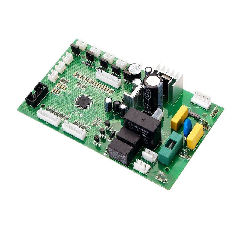
What is Through-Hole Technology?
Through-hole technology is an older method of electronic component insertion and mounting. It involves drilling holes in the PCB surface to mount the components. This method needs larger space on the PCB, and it's heavier in weight. One significant advantage of through-hole technology is that it can handle more substantial power as the components are securely held in place.What is Surface Mount Technology?
Surface Mount Technology (SMT) is a more modern technique of mounting electronic components onto the PCB surface. SMT components are smaller, lighter in weight, and not suited to handling vast power surges. SMT's significant advantage is, it's take up less space, consumes less material and is less expensive than through-hole.Pros and Cons of through-hole and Surface Mount Technology
Through-hole technology offers many advantages, such as handling more significant power surges, more durable assembly, and enabling the use of larger components. However, through-hole assembly also comes with downsides, such as increased weight and size, higher manufacturing costs, and more challenging repairs. SMT offers many advantages, such as taking up less space, less expensive manufacturing, and lighter weight. Downsides, however, include the inability to handle heavy power surges, weaker solder joints, and more challenging placement and alignment of components.Conclusion
PCB Design and Layout is the heart of any electronic device. It plays a vital role in determining the performance of the electronic components on the Printed Circuit Board. Each PCB design method has its benefits and drawbacks, and it's up to the designer to determine which method is best for a specific application. Shenzhen Hi Tech Co., Ltd. is a leading PCB manufacturer dedicated to providing on-time delivery and high-quality PCB products to customers worldwide. We possess advanced technology, strict QC management, and efficient customer services. Contact us at Dan.s@rxpcba.com for more information.Research Papers on PCB Design and Layout:
Chan, C. T., Chan, K. W., & Tam, H. Y. (2016). PCB design of low-cost UWB antenna for RFID applications. IEEE Antennas and Wireless Propagation Letters, 15, 1113-1116.
Chen, Y., Wang Yang, J., & Cai, W. (2016). Design and Development of a Rapid Prototyping Printed Circuit Board (PCB) Plotter. In 2016 11th International Conference on Computer Science & Education (ICCSE) (pp. 149-152). IEEE.
Ciesla, T., & Habrych, M. (2016). The New Trend for Environmentally Friendly Printed Circuit Board Design. In 2016 International Conference on Military Communications and Information Systems (ICMCIS) (pp. 1-6). IEEE.
Kondrasenko, I., & Radaev, R. (2015). The comparison of the productivity of PCB design using different integrated circuit design software. In 2015 IEEE Conference on Quality Management, Transport and Information Security, Information Technologies (IT& MQ&IS) (pp. 21-24). IEEE.
Qi, Y., & Chen, K. (2016). Research on design of electronic ruler for PCB terminal width. In 2016 IEEE Advanced Information Management,Communicates,Electronic and Automation Control Conference (IMCEC) (pp. 269-272). IEEE.
Sato, K., & Nakachi, A. (2016). Development of a new PCB design rule and DFM methodology for the space environment. In 2016 Asia-Pacific International Symposium on Aerospace Technology (APISAT) (pp. 566-574). IEEE.
Shao, J., Pan, L., Wu, K., Hu, X., & Zhao, Y. (2016). Research on Key Technologies of 3D Printed Mold to Accelerate MEMS PCB Prototype. In 2016 IEEE International Conference on Mechatronics and Automation (ICMA) (pp. 192-197). IEEE.
Wang, Y. (2016). Design and Manufacture of Automated PCB Reworking System. In 2016 13th International Conference on Ubiquitous Robots and Ambient Intelligence (URAI) (pp. 283-285). IEEE.
Wu, H., Zhu, H., & Qu, F. (2015). Multiple RC time constant ensemble PCB modeling method. In 2015 IEEE International Conference on Industrial Informatics-Computing Technology, Intelligent Technology, Industrial Information Integration (ICIICII) (pp. 11-14). IEEE.
Yang, M., Li, L., Chen, L., Chen, X., & Chen, P. (2015). Analysis on PCB design based on the electromagnetic coupling theory. In 2015 IEEE 2nd International Conference on Electronic Information and Communication Technology (ICEICT) (pp. 29-32). IEEE.
Yuan, D., Chen, H., Zhao, H., & Zhang, L. (2016). PCB Finite Element Analysis and Experimental Verification of 3D Printer with Delta Structure. In 2016 IEEE International Conference on Mechatronics and Automation (ICMA) (pp. 758-762). IEEE.